MNF | Micro Nano Facility
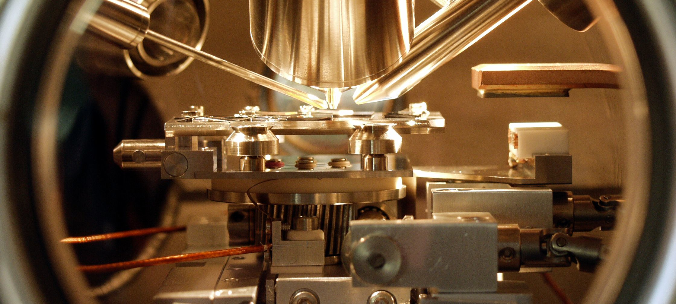
The Micro and Nano Characterization and Fabrication (MNF) facility is a state-of-the-art facility dedicated to pushing semiconductor technology beyond its current state. The facility specializes in silicon micro and nanoprocessing and produces leading-edge sensors through its worldwide recognized competencies in optical and electronic lithography, etching, physical vapor deposition (PVD), chemical vapor deposition (CVD), ion implantation, and thermal processes.
Opportunities in MNF
The MNF facility, with more than 1000 sq meters of ISO4-ISO6 clean rooms and other 1000 sq meters of laboratories, offers fully controlled process modules that allow for customization of several technological platforms, such as SDD, SiPM, LGAD, opto sensors, and gas sensors, for various applications, including space and other harsh environments. The facility also engages in quantum technologies and nanofabrication research and development based on focused ion beam (FIB) and scanning electron microscope (SEM) innovative tools.
In addition to fabrication, the facility offers testing and analytical laboratories for materials and device characterization, packaging, and integration laboratories in coordination with the other units for developing full systems at different technology readiness levels (TRLs).
MNF is an open infrastructure equipped to accommodate both external users from research and industry.
ISO certified
The MNF laboratories are ISO certified ISO 9001:2015 since 2012, ensuring that all processes meet international standards for quality and safety. From 2024, the ISO 9001:2015 certification has been extended to the SD center, together with the other centers of FBK. (FBK certificate – SD certificate)
From 2024, MNF and all FBK have also received ISO/IEC 27001:2022 certification. (FBK certificate – SD certificate)
