Equipment | MTSD
-
![]() XPSXPS is based on the photoelectric effect. The interaction between electromagnetic radiation with matter can generate the emission of an electron (called photoelectron). Photoelectron energy measurement allows to obtain several information. XPS is a nondestructive technique. It can provide information about surface layers or thin-film structures. Identification and quantification of elements it is also achievable in the detection limit range The instrument operating in FBK is a Kratos Axis-Ultra
XPSXPS is based on the photoelectric effect. The interaction between electromagnetic radiation with matter can generate the emission of an electron (called photoelectron). Photoelectron energy measurement allows to obtain several information. XPS is a nondestructive technique. It can provide information about surface layers or thin-film structures. Identification and quantification of elements it is also achievable in the detection limit range The instrument operating in FBK is a Kratos Axis-Ultra -
![]() ToF-SIMSTime-of-Flight Secondary Ion Mass Spectrometry (ToF-SIMS) is a surface-sensitive analytical technique that uses a pulsed ion beam to eject secondary ions from a sample's surface, which are then analyzed based on their time-of-flight to determine mass-to-charge ratios. It provides high-resolution chemical and molecular imaging of surfaces, detecting trace elements, organic compounds, and contaminants in materials such as semiconductors, polymers, and biological samples. The technique offers ultra-high sensitivity, spatial resolution in the nanometer range, and the ability to analyze both elemental and molecular species without significant damage to the sample. The instrument operating in FBK is a ToV-SIMS IV and in one year will be replaced by state of art a TOF-SIMS M6.
ToF-SIMSTime-of-Flight Secondary Ion Mass Spectrometry (ToF-SIMS) is a surface-sensitive analytical technique that uses a pulsed ion beam to eject secondary ions from a sample's surface, which are then analyzed based on their time-of-flight to determine mass-to-charge ratios. It provides high-resolution chemical and molecular imaging of surfaces, detecting trace elements, organic compounds, and contaminants in materials such as semiconductors, polymers, and biological samples. The technique offers ultra-high sensitivity, spatial resolution in the nanometer range, and the ability to analyze both elemental and molecular species without significant damage to the sample. The instrument operating in FBK is a ToV-SIMS IV and in one year will be replaced by state of art a TOF-SIMS M6. -
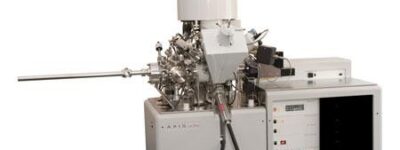
![]() SIMSAtoms or groups of atoms are etched by a primary ion beam (0.25÷20keV). A small fraction of these (typically 1%) is ionized and can therefore be analyzed according to the mass/charge ratio. Typical performances of the SIMS technique are the ability to detect each isotope of the periodic table with detection limits ranging from 1ppm to 1ppb, a mass resolution M/ΔM up to 20000, a lateral resolution of the order of 1µm and a depth resolution at nm range. The instrument in FBK laboratories is a CAMECA SC-Ultra.
SIMSAtoms or groups of atoms are etched by a primary ion beam (0.25÷20keV). A small fraction of these (typically 1%) is ionized and can therefore be analyzed according to the mass/charge ratio. Typical performances of the SIMS technique are the ability to detect each isotope of the periodic table with detection limits ranging from 1ppm to 1ppb, a mass resolution M/ΔM up to 20000, a lateral resolution of the order of 1µm and a depth resolution at nm range. The instrument in FBK laboratories is a CAMECA SC-Ultra. -
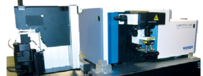
![]() Confocal Raman SpectrometerConfocal Raman spectroscopy and imaging deliver precise chemical insights into nanomaterials with sub-micron spatial resolution. The HORIBA Scientific LabRAM HR is operating at FBK laboratories. It is an Evolution spectrometer, seamlessly integrated with SPM Scanning Probe Microscope, which provides a highly versatile and reliable platform for simultaneous co-localized Raman-AFM and TERS measurements. Tip-enhanced Raman Spectroscopy (TERS) combines the chemical specificity of Raman spectroscopy with ultra-high spatial resolution, typically reaching 10 nm. Additionally, the system can be used for standalone Raman or AFM measurements. Laser ranges: Lasers: 355 / 532 / 633 / 785 nm;
Confocal Raman SpectrometerConfocal Raman spectroscopy and imaging deliver precise chemical insights into nanomaterials with sub-micron spatial resolution. The HORIBA Scientific LabRAM HR is operating at FBK laboratories. It is an Evolution spectrometer, seamlessly integrated with SPM Scanning Probe Microscope, which provides a highly versatile and reliable platform for simultaneous co-localized Raman-AFM and TERS measurements. Tip-enhanced Raman Spectroscopy (TERS) combines the chemical specificity of Raman spectroscopy with ultra-high spatial resolution, typically reaching 10 nm. Additionally, the system can be used for standalone Raman or AFM measurements. Laser ranges: Lasers: 355 / 532 / 633 / 785 nm; -
![]() FIB-STEMFocused Ion Beam Scanning Transmission Electron Microscopy (FIB-STEM) is an advanced technique that combines precise ion beam milling with high-resolution electron imaging. It enables site-specific sample preparation and atomic-scale characterization of materials, making it ideal for studying nanoscale structures, defects, and interfaces in semiconductors, metals, and biological specimens. The equipment in FBK laboratories is a Thermo Fisher Helios™ 5 PFIB CXE. Equipment with a Xe ion source, it can provide 20 nm structures. The detectors are: secondary TLD-SE; Backscattered: TLD-BSE; STEM. The instrument is also equipped by EDS and EBSD thechniques.
FIB-STEMFocused Ion Beam Scanning Transmission Electron Microscopy (FIB-STEM) is an advanced technique that combines precise ion beam milling with high-resolution electron imaging. It enables site-specific sample preparation and atomic-scale characterization of materials, making it ideal for studying nanoscale structures, defects, and interfaces in semiconductors, metals, and biological specimens. The equipment in FBK laboratories is a Thermo Fisher Helios™ 5 PFIB CXE. Equipment with a Xe ion source, it can provide 20 nm structures. The detectors are: secondary TLD-SE; Backscattered: TLD-BSE; STEM. The instrument is also equipped by EDS and EBSD thechniques. -
![]() SEMThe FBK laboratories are also equipped with a Thermofisher Phenom XL G2 Desktop SEM. This instrument allows to: - Obtain high-quality information to discover failures early and rapidly adjust the production process when needed. - Automate quality control to process a high volume of samples with fewer chances of human error. - Get up to speed quickly with an all-new, easy-to-learn interface ideal for a wide range of applications. The instrument is equipped with long-lifetime CeB₆ (cerium hexaboride) source to obtain high quality images with many details. Also EDX analyses are possible
SEMThe FBK laboratories are also equipped with a Thermofisher Phenom XL G2 Desktop SEM. This instrument allows to: - Obtain high-quality information to discover failures early and rapidly adjust the production process when needed. - Automate quality control to process a high volume of samples with fewer chances of human error. - Get up to speed quickly with an all-new, easy-to-learn interface ideal for a wide range of applications. The instrument is equipped with long-lifetime CeB₆ (cerium hexaboride) source to obtain high quality images with many details. Also EDX analyses are possible -
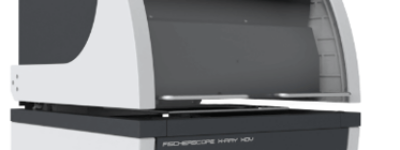
![]() XRFThe X-RAY XDVµ HF is a high-performance X-ray fluorescence (XRF) spectrometer designed for non-destructive, high-resolution elemental analysis. It utilizes a focused X-ray beam to measure thin films, coatings, and material compositions with excellent precision. Applications: - Thickness and composition analysis of coatings in electronics and semiconductor industries. - Quality control in metal plating and material research. - Trace element detection in environmental and geological samples.
XRFThe X-RAY XDVµ HF is a high-performance X-ray fluorescence (XRF) spectrometer designed for non-destructive, high-resolution elemental analysis. It utilizes a focused X-ray beam to measure thin films, coatings, and material compositions with excellent precision. Applications: - Thickness and composition analysis of coatings in electronics and semiconductor industries. - Quality control in metal plating and material research. - Trace element detection in environmental and geological samples.